EN
EN
Quick Links
The semiconductor industry is the cornerstone of modern technology, and its manufacturing process represents the highest level of precision control in today's industrial world. As nanoscale process nodes continue to achieve new breakthroughs, the internal space of semiconductor production equipment has become extremely valuable, placing incredibly stringent demands on the size, precision, and reliability of motion control components. Against this backdrop, the MGN3 miniature linear guide, with its ultra-compact design and exceptional guiding performance, has become an indispensable "precision skeleton" in numerous high-end semiconductor machines.
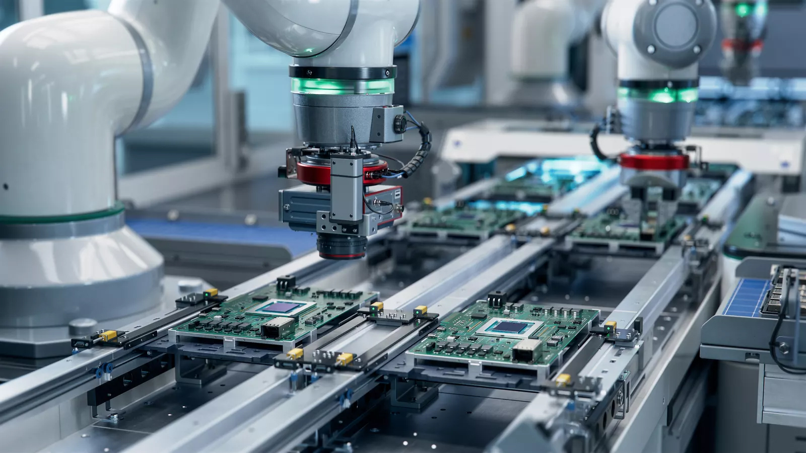
The internal structures of semiconductor manufacturing equipment (such as lithography machines, etching systems, and wafer inspection equipment) are exceptionally complex. Traditional standard linear guides are often too bulky to fit into these confined installation spaces. As an ultra-small specification within the miniature guide series, the MGN3 offers the following irreplaceable advantages:
Ultra-Compact Size: The MGN3 features an extremely small cross-sectional profile, providing stable linear motion within highly restricted spaces. This offers tremendous freedom for the miniaturization and integrated design of equipment.
High Precision and Smoothness: During the processing and inspection of semiconductor wafers, even the slightest vibration or positioning deviation can lead to the scrapping of an entire wafer. Through an optimized ball circulation design and ultra-high-precision grinding processes, the MGN3 guide ensures sub-micron positioning accuracy and exceptionally smooth motion trajectories.
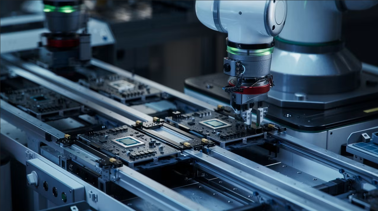
As wafers are transferred from one processing chamber to another, robotic arms must perform highly precise and stable extensions and vertical movements. MGN3 miniature guides are frequently integrated into the end effectors or miniature clamps of wafer-handling robots to ensure absolute stability during grasping and placement, thereby preventing edge damage.
In back-end packaging processes, wire bonders must perform bonding operations at extremely high frequencies. The lightweight nature of the MGN3 guide reduces the inertia of moving parts, allowing it to perfectly adapt to high-frequency, high-acceleration reciprocating motions while maintaining superior bonding alignment accuracy.
Semiconductor defect inspection equipment relies on high-resolution optical lenses to scan wafer surfaces. MGN3 guides are widely used in the Z-axis and XY-axis fine-tuning mechanisms of optical probes and miniature stages. This guarantees absolute smoothness during focusing and scanning, preventing image blur caused by mechanical vibrations.
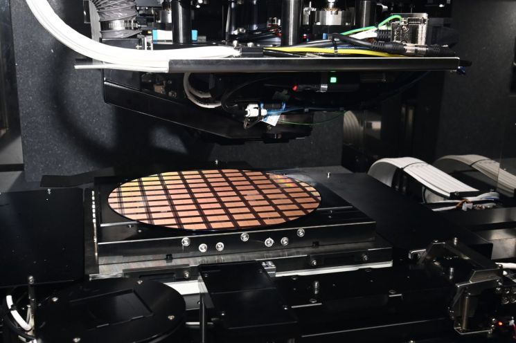
Semiconductor manufacturing typically takes place in ultra-high vacuum (UHV) environments or high-class cleanrooms, where standard miniature guides cannot meet the stringent requirements for dust prevention, anti-static properties, and corrosion resistance. Therefore, deep customization of MGN3 guides has become a core consideration for semiconductor equipment manufacturers during procurement:
Strict Material Selection: Semiconductor applications universally require the use of high-grade stainless steel to ensure that the guide not only possesses high rigidity but also achieves extremely low particle generation in cleanroom environments.
Customized Mounting Holes and Dimensions: To perfectly accommodate the non-standard equipment designs of various customers, customizing the mounting hole diameters and specific block dimensions of the MGN3 guide can greatly simplify the equipment assembly process and improve overall efficiency.
Zero "Flaking" Risk to Guarantee Ultimate Cleanliness: Semiconductor wafer manufacturing has zero tolerance for micro-dust particles. Any applied anti-corrosion surface coatings carry the hidden risk of microscopic flaking under high-frequency reciprocating mechanical friction. By operating directly with a pure stainless steel body, the MGN3 fundamentally eliminates the possibility of coating flaking that could contaminate vacuum chambers or wafers.
As semiconductor processes advance toward even smaller nanoscale nodes, the demand for the miniaturization and customization of core equipment components will continue to explode. The MGN3 miniature linear guide is not merely a standardized transmission component, but a highly customizable precision platform capable of deep optimization (e.g., custom hole dimensions and surface treatments) based on the specific needs of semiconductor clients. Through high-quality machining and rigorous attention to detail, the MGN3 will continue to provide solid and reliable support for the iterative upgrades of the global semiconductor industry.