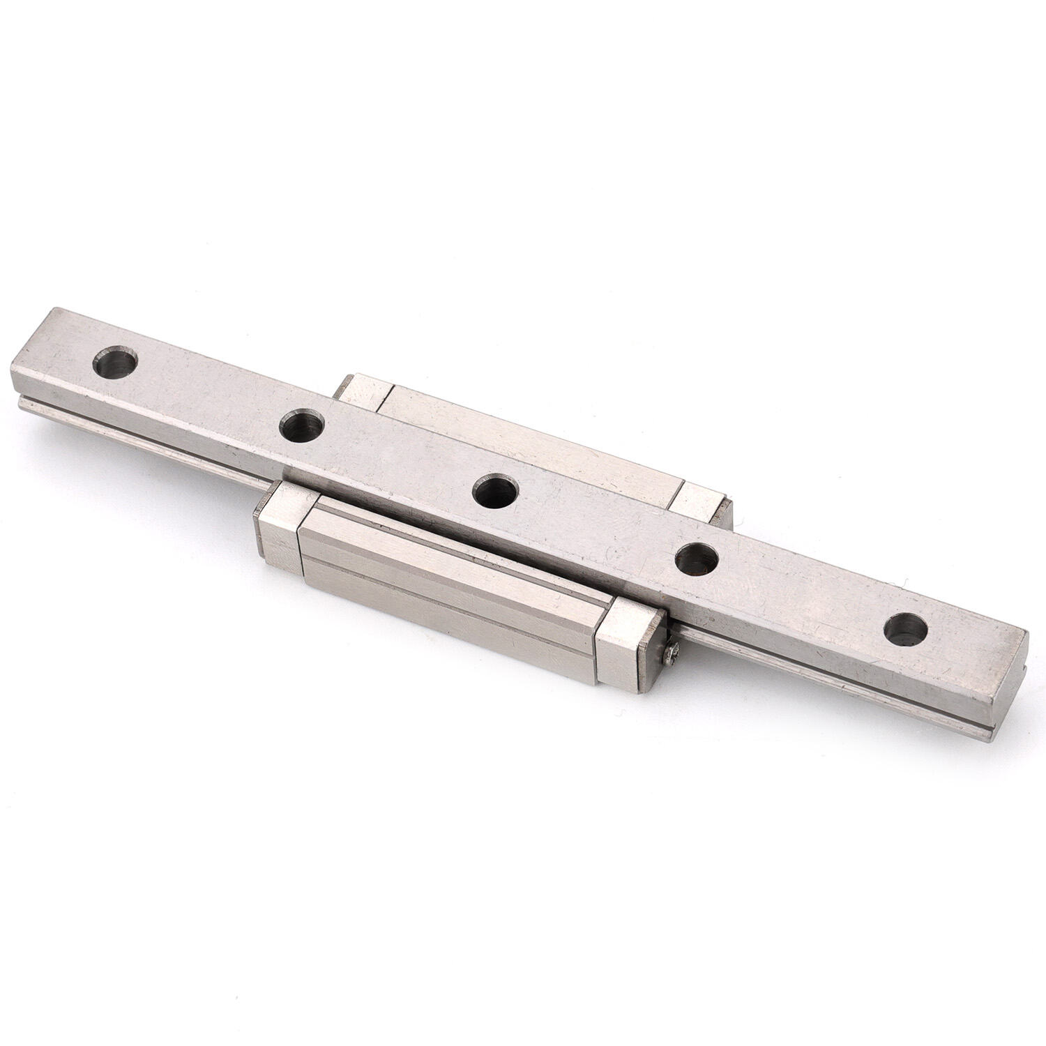
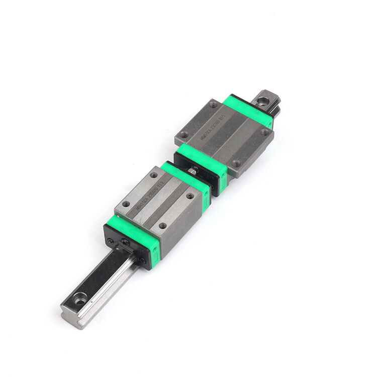
La fabricación de semiconductores representa uno de los entornos de precisión más exigentes de la industria moderna, donde las tolerancias de los componentes, medidas en nanómetros, pueden determinar el éxito o el fracaso de líneas de producción enteras. En este entorno riguroso, guía lineal los rieles constituyen la columna vertebral fundamental de los sistemas automatizados de posicionamiento, los equipos de manipulación de obleas y las máquinas de ensamblaje de precisión que impulsan la fabricación de semiconductores. Los requisitos de rendimiento para estos componentes críticos van mucho más allá de las aplicaciones industriales estándar, exigiendo características superficiales, precisión dimensional y resistencia a la contaminación que solo pueden lograrse mediante procesos especializados de electrodeposición diseñados específicamente para entornos semiconductor.
Los procesos personalizados de electrodeposición han surgido como la solución definitiva para satisfacer estas demandas de precisión sin precedentes, transformando los estándares guías lineales en componentes de grado semiconductor capaces de soportar las operaciones más críticas del sector. Estas tecnologías avanzadas de recubrimiento abordan simultáneamente múltiples desafíos, como la reducción de la generación de partículas, la mejora de la resistencia a la corrosión, la mejora de la estabilidad dimensional y la prevención de la contaminación, aspectos que los tratamientos superficiales tradicionales simplemente no pueden igualar. Comprender cómo estos procesos especializados de galvanoplastia permiten que los rieles de guía lineal cumplan con los exigentes requisitos de precisión del sector semiconductor revela la ingeniería sofisticada necesaria para respaldar las capacidades de fabricación de chips de próxima generación.
Desafíos del entorno semiconductor para los sistemas de movimiento lineal
Requisitos de control de contaminación en salas limpias
Los entornos de salas limpias para semiconductores imponen normas rigurosas de control de contaminación que afectan directamente el diseño y el tratamiento superficial de los rieles de guía lineal utilizados en equipos críticos de fabricación. La generación de partículas por componentes mecánicos móviles representa una amenaza constante para la calidad de los obleas y las tasas de rendimiento, lo que exige que los rieles de guía lineal demuestren una lisura superficial excepcional y una estabilidad material bajo funcionamiento continuo. Los procesos personalizados de electrodeposición abordan estas preocupaciones relacionadas con la contaminación al crear capas superficiales ultra-lisas y no desprendibles que minimizan la generación de partículas, manteniendo al mismo tiempo la integridad estructural necesaria para aplicaciones de posicionamiento de precisión.
El enfoque de galvanoplastia para aplicaciones en el sector de semiconductores implica típicamente varias capas de recubrimiento, cada una diseñada para abordar vías específicas de contaminación que podrían comprometer la integridad de la sala limpia. Las capas base se centran en la resistencia a la corrosión y la estabilidad dimensional, mientras que los recubrimientos intermedios aportan resistencia al desgaste y propiedades de endurecimiento superficial esenciales para una larga vida útil. La capa superficial final recibe un tratamiento especializado para lograr el acabado tipo espejo y la inercia química requeridos en operaciones en salas limpias Clase 1 y Clase 10, donde incluso las irregularidades superficiales microscópicas pueden generar niveles inaceptables de partículas.
Estabilidad dimensional bajo ciclos térmicos
Los ciclos térmicos representan otro desafío significativo para los rieles de guía lineal que operan en entornos de fabricación de semiconductores, donde las temperaturas de proceso pueden variar drásticamente durante distintas etapas de fabricación. Los rieles de guía lineal estándar pueden experimentar cambios dimensionales que comprometen la precisión y la repetibilidad del posicionamiento, especialmente cuando soportan sistemas de manipulación de obleas o equipos de litografía que requieren una precisión a nivel de nanómetro. Los procesos personalizados de electrodeposición abordan las preocupaciones relacionadas con la estabilidad térmica mediante la incorporación de materiales de recubrimiento cuyos coeficientes de expansión térmica están adaptados y que poseen propiedades de alivio de tensiones, lo que mantiene la integridad dimensional a lo largo de los rangos de temperatura de operación.
Las formulaciones avanzadas de galvanoplastia para aplicaciones en el sector semiconductor suelen incluir composiciones especiales de aleaciones que ofrecen una estabilidad térmica superior frente a los sistemas convencionales de cromado o niquelado. Estos recubrimientos personalizados se someten a un tratamiento térmico controlado durante el proceso de galvanoplastia, generando patrones de tensión residual que contrarrestan los efectos de la dilatación térmica y mantienen una geometría constante de las guías bajo distintas condiciones de temperatura. Esta estabilidad dimensional permite que las guías lineales soporten los requisitos de posicionamiento de precisión, incluso cuando operan en entornos sometidos a ciclos térmicos significativos.
Resistencia química y compatibilidad con gases de proceso
Los procesos de fabricación de semiconductores exponen los rieles de guía lineal a entornos químicos agresivos, incluidos gases de proceso, disolventes de limpieza y compuestos de grabado que pueden degradar rápidamente los tratamientos superficiales estándar y comprometer la fiabilidad del equipo. Los procesos personalizados de galvanoplastia para aplicaciones en el sector de los semiconductores deben demostrar compatibilidad con fluoruro de hidrógeno, amoníaco, gases a base de cloro y otros compuestos reactivos comúnmente utilizados en los procesos de fabricación de chips. La selección de la química de galvanoplastia resulta crítica para garantizar un rendimiento a largo plazo y prevenir problemas de contaminación que podrían afectar la calidad de los obleas o el tiempo de actividad del equipo.
Las formulaciones especializadas de galvanoplastia incorporan aleaciones resistentes a la corrosión y recubrimientos barrera que ofrecen una inercia química excepcional, manteniendo al mismo tiempo las propiedades mecánicas requeridas para aplicaciones de movimiento lineal. Estos recubrimientos avanzados se someten a extensas pruebas de compatibilidad con productos químicos específicos del proceso para verificar su rendimiento en condiciones reales de operación, garantizando así que las guías lineales conserven sus características de precisión durante largos períodos de exposición a entornos químicos agresivos. La resistencia química resultante permite a los fabricantes de equipos para la industria de semiconductores especificar guías lineales con total confianza en aplicaciones exigentes, donde la fiabilidad del equipo afecta directamente al rendimiento de producción y al tiempo de actividad de la instalación.
Desarrollo personalizado del proceso de galvanoplastia
Preparación de la superficie y análisis del sustrato
El galvanizado personalizado exitoso para rieles de guía lineal de grado semiconductor comienza con un análisis exhaustivo del sustrato y protocolos de preparación superficial que garantizan una adherencia óptima del recubrimiento y sus características de rendimiento. La composición del material base, el perfil de rugosidad superficial y los patrones de tensión existentes influyen todos en el diseño del proceso de galvanizado y en las propiedades finales del recubrimiento obtenidas sobre los rieles de guía lineal. Técnicas avanzadas de análisis superficial, como la microscopía electrónica y la perfilometría, orientan el desarrollo de procedimientos de preparación específicos para cada sustrato, maximizando la uniformidad del recubrimiento y minimizando los defectos relacionados con tensiones que podrían comprometer el rendimiento de precisión.
La preparación de la superficie para aplicaciones en el sector de los semiconductores generalmente implica varias etapas de limpieza, acondicionamiento mecánico y pasos de activación química diseñados para eliminar contaminantes y crear condiciones óptimas de unión para las capas posteriores de electrodeposición. Cada etapa de preparación se optimiza cuidadosamente según las características específicas esquinas de guía lineal de la geometría y las propiedades del material, garantizando una calidad uniforme del recubrimiento en perfiles complejos de rieles y superficies de rodamiento. El proceso de preparación también aborda las tensiones residuales generadas durante la fabricación, que podrían interactuar con las tensiones inducidas por la electrodeposición y afectar la estabilidad dimensional de los componentes terminados.
Diseño de la arquitectura de recubrimiento multicapa
Los procesos personalizados de galvanoplastia para rieles lineales de guía de semiconductores suelen emplear arquitecturas sofisticadas de recubrimientos multicapa que abordan distintos requisitos de rendimiento mediante funciones y composiciones especializadas de cada capa. El diseño del sistema de recubrimiento comienza con capas base promotoras de adherencia, que garantizan una fuerte unión al material del sustrato y establecen una base para los recubrimientos funcionales posteriores. Las capas intermedias se centran en propiedades mecánicas, como dureza, resistencia al desgaste y capacidad de soporte de carga, mientras que las capas superficiales enfatizan la resistencia a la contaminación, la inercia química y las características de fricción esenciales para el funcionamiento en salas limpias.
La optimización del espesor de capa representa un aspecto crítico del diseño de la arquitectura de recubrimientos, equilibrando los requisitos de rendimiento con las tolerancias dimensionales y las consideraciones de gestión de tensiones. Cada capa de recubrimiento se optimiza individualmente en cuanto a su composición, parámetros de deposición y procedimientos de posprocesamiento para lograr las propiedades deseadas sin comprometer el rendimiento general del sistema. La estructura multicapa resultante proporciona rieles de guía lineal con características de rendimiento superiores a las de los enfoques de una sola capa, manteniendo al mismo tiempo la precisión dimensional requerida para aplicaciones de posicionamiento en el sector semiconductor.
Optimización y control de parámetros del proceso
La optimización de los parámetros del proceso de galvanoplastia para rieles lineales de semiconductores requiere un control preciso de la densidad de corriente, la temperatura de la cuba, los patrones de agitación y la composición química durante todo el ciclo de deposición del recubrimiento. Estos parámetros influyen directamente en la uniformidad del recubrimiento, la resistencia de adherencia, los niveles de tensión interna y la calidad del acabado superficial, factores que determinan las características finales de rendimiento de los componentes tratados. Los sistemas avanzados de control de procesos supervisan y ajustan simultáneamente múltiples parámetros para mantener una calidad constante del recubrimiento en todos los lotes de producción, adaptándose además a las geometrías complejas típicas de los conjuntos de rieles lineales.
Los protocolos de control de calidad para procesos personalizados de galvanoplastia incluyen la monitorización en tiempo real de la química del baño, las mediciones del espesor del recubrimiento y la verificación del acabado superficial para garantizar el cumplimiento de las especificaciones de la industria de semiconductores. Los métodos de control estadístico de procesos registran las variaciones de los parámetros y las métricas de calidad del recubrimiento con el fin de identificar oportunidades de optimización y prevenir desviaciones de calidad que podrían afectar el rendimiento de los rieles lineales de guía en aplicaciones críticas. El enfoque integral de control de procesos permite la producción consistente de guías lineales de grado semiconductor que cumplen con los exigentes requisitos de las instalaciones modernas de fabricación de chips.
Beneficios de rendimiento y ventajas de aplicación
Mejora de la precisión y de la repetibilidad
Los procesos personalizados de galvanoplastia aportan mejoras medibles en la precisión de los rieles guía lineales utilizados en aplicaciones semiconductoras, con mejoras en el acabado superficial que se traducen directamente en una reducción de los errores de posicionamiento y un rendimiento mejorado en cuanto a repetibilidad. La rugosidad superficial controlada lograda mediante galvanoplastia especializada permite que los rieles guía lineales mantengan características de fricción constantes y eliminen los fenómenos de microadherencia que pueden comprometer la precisión de posicionamiento en aplicaciones a escala nanométrica. Estas mejoras de precisión resultan especialmente críticas en sistemas de paso de obleas (wafer steppers), estaciones de prueba (probe stations) y equipos de ensamblaje, donde los errores de posicionamiento afectan directamente las tasas de rendimiento (yield) y la capacidad del proceso.
Los tratamientos superficiales por electrodeposición también ofrecen una consistencia geométrica superior en los conjuntos de rieles guía lineales, minimizando las variaciones en rectitud, paralelismo y perfil superficial que podrían acumularse en errores de posicionamiento significativos a lo largo de grandes recorridos. La uniformidad del proceso de recubrimiento garantiza que varios rieles guía lineales dentro de un mismo sistema presenten características de rendimiento coincidentes, lo que permite un movimiento coordinado en múltiples ejes con la precisión requerida para los avanzados procesos de fabricación de semiconductores. La estabilidad dimensional a largo plazo proporcionada por la electrodeposición personalizada mantiene estas ventajas de precisión durante ciclos operativos prolongados, respaldando un rendimiento constante del equipo a lo largo de los ciclos de vida típicos de las herramientas para semiconductores.
Vida útil extendida y mantenimiento reducido
La galvanoplastia de grado semiconductor extiende significativamente la vida útil operativa de los rieles de guía lineal al ofrecer una resistencia al desgaste y una protección contra la corrosión superiores en comparación con los tratamientos superficiales convencionales o los componentes sin recubrimiento. La mayor durabilidad reduce los requisitos de mantenimiento y la frecuencia de sustitución de componentes, minimizando el tiempo de inactividad del equipo y cumpliendo con las exigentes demandas de disponibilidad elevada propias de las operaciones de fabricación de semiconductores. Las formulaciones avanzadas de galvanoplastia presentan tasas de desgaste varias órdenes de magnitud inferiores a las de los tratamientos convencionales, lo que permite que los rieles de guía lineal mantengan un rendimiento preciso durante millones de ciclos operativos sin degradación.
La extensión de los intervalos de mantenimiento ofrece importantes beneficios económicos para las instalaciones semiconductoras, donde los costes derivados de la inactividad de los equipos pueden superar miles de dólares por hora y las ventanas programadas para el mantenimiento requieren una coordinación cuidadosa con los horarios de producción. Las guías lineales galvanizadas personalizadas mantienen sus características de rendimiento con requisitos mínimos de lubricación y menor sensibilidad a la acumulación de contaminantes, simplificando los procedimientos de mantenimiento y alargando los intervalos entre intervenciones importantes. Las mejoras en fiabilidad permiten a los fabricantes de semiconductores optimizar la utilización de los equipos, manteniendo al mismo tiempo los estándares de precisión esenciales para una producción competitiva de chips.
Resistencia a la contaminación y compatibilidad con salas limpias
Los procesos especializados de galvanoplastia crean superficies de rieles guía lineales con una excepcional resistencia a la contaminación, evitando la acumulación de partículas, residuos químicos y otros contaminantes que podrían comprometer la integridad de las salas limpias o el rendimiento del equipo. Las características de superficie lisa e inerte químicamente logradas mediante galvanoplastia personalizada resisten la adherencia de partículas y permiten una limpieza eficaz utilizando disolventes y procedimientos estándar compatibles con la industria semiconductor. Esta resistencia a la contaminación resulta esencial para los rieles guía lineales que soportan procesos críticos, como la manipulación de obleas, el alineamiento de máscaras y el ensamblaje de dispositivos, donde el control de la contaminación impacta directamente en la calidad del producto.
La compatibilidad con salas limpias va más allá de la resistencia a la contaminación e incluye características de desgasificación, niveles de contaminación iónica y propiedades de generación de partículas que deben cumplir requisitos rigurosos de la instalación. Los procesos personalizados de electrodeposición someten a ensayos de validación para verificar su compatibilidad con clasificaciones específicas de salas limpias y con los requisitos del proceso, garantizando así que las guías lineales tratadas contribuyan a los estándares generales de limpieza de la instalación, en lugar de comprometerlos. El rendimiento validado en salas limpias permite a los fabricantes de semiconductores especificar guías lineales electrodepositadas con confianza, incluso en los entornos de fabricación más exigentes.
Consideraciones de Implementación y Buenas Prácticas
Desarrollo de especificaciones y selección de proveedores
La implementación exitosa de la galvanoplastia personalizada para rieles lineales de guía para semiconductores requiere el desarrollo integral de especificaciones que aborden tanto los requisitos de rendimiento funcional como las consideraciones de compatibilidad con la fabricación. Las especificaciones del equipo deben definir claramente las tolerancias dimensionales, los requisitos de acabado superficial, los parámetros de resistencia química y las normas de control de contaminación que debe cumplir el proceso de galvanoplastia. La colaboración entre los fabricantes de equipos, los proveedores de galvanoplastia y los usuarios finales de semiconductores garantiza que las especificaciones respondan a las condiciones reales de operación y a los requisitos de rendimiento, en lugar de limitarse a estándares industriales genéricos que podrían no reflejar las demandas específicas de la aplicación.
Los criterios de selección de proveedores deben hacer hincapié en la experiencia demostrada en aplicaciones de semiconductores, el cumplimiento de los sistemas de calidad y las capacidades de desarrollo de procesos que respalden los requisitos de formulación personalizada. Los proveedores calificados de electrodeposición suelen mantener la certificación ISO 9001, disponer de instalaciones limpias y contar con laboratorios de ensayo equipados para verificar los parámetros de rendimiento específicos de los semiconductores. El proceso de evaluación de proveedores debe incluir auditorías de instalaciones, evaluaciones de la capacidad de los procesos e instalaciones de referencia que demuestren la implementación exitosa de proyectos similares de electrodeposición para aplicaciones en el sector de los semiconductores.
Protocolos de control de calidad y ensayo
Protocolos rigurosos de aseguramiento de la calidad garantizan que las guías lineales galvanizadas personalizadas cumplan de forma constante con los requisitos de rendimiento para la industria semiconductora durante todo su ciclo de producción y de funcionamiento. Los procedimientos de ensayo deben abordar la uniformidad del espesor del recubrimiento, la resistencia a la adherencia, la calidad del acabado superficial y la resistencia a la contaminación, utilizando técnicas de medición trazables a normas reconocidas. Los protocolos de ensayo acelerado simulan las condiciones de operación y brindan confianza en las proyecciones de rendimiento a largo plazo, mientras que los procedimientos de inspección de entrada verifican el cumplimiento de las especificaciones antes de la instalación en equipos críticos para la industria semiconductora.
Los métodos de control estadístico de la calidad supervisan las variaciones del proceso y las tendencias de rendimiento para identificar posibles problemas antes de que afecten a la calidad de la producción o a la fiabilidad del equipo. Las pruebas periódicas de muestras de producción mantienen el control del proceso y proporcionan una advertencia temprana sobre desviaciones de los parámetros o cambios en el rendimiento de los proveedores que podrían afectar a la calidad de los rieles de guía lineal. Los requisitos de documentación para aplicaciones en el sector semiconductor suelen superar las prácticas industriales estándar, exigiendo registros detallados de trazabilidad, certificados de ensayo y datos de validación de procesos que respalden el cumplimiento de los estándares de calidad del sector semiconductor.
Integración con el diseño y el mantenimiento de equipos
La integración óptima de rieles lineales galvanizados personalizados requiere la coordinación entre las especificaciones del recubrimiento, los requisitos de diseño del equipo y los procedimientos de mantenimiento para maximizar los beneficios de rendimiento y minimizar, al mismo tiempo, la complejidad de la implementación. Los aspectos a considerar en el diseño incluyen la compatibilidad con los lubricantes, la compensación de la dilatación térmica y la accesibilidad para las actividades de inspección y mantenimiento que puedan ser necesarias durante el funcionamiento del equipo. La participación temprana de especialistas en galvanoplastia en las fases de diseño del equipo permite optimizar las especificaciones del recubrimiento según las condiciones operativas específicas y los requisitos de mantenimiento.
El desarrollo de los procedimientos de mantenimiento debe tener en cuenta las características específicas de las superficies galvanizadas, incluidos los métodos adecuados de limpieza, los requisitos de lubricación y las técnicas de inspección que preserven la integridad del recubrimiento sin comprometer el rendimiento del equipo. Los programas de formación para el personal de mantenimiento garantizan la manipulación y el cuidado adecuados de los rieles guía lineales galvanizados, evitando daños que podrían afectar su precisión o su resistencia a la contaminación. El enfoque integrado de diseño, recubrimiento y mantenimiento permite a los fabricantes de semiconductores aprovechar al máximo los beneficios de sus inversiones en galvanoplastia personalizada, manteniendo al mismo tiempo la eficiencia operativa y la fiabilidad del equipo.
Preguntas frecuentes
¿Qué hace necesaria la galvanoplastia para los rieles guía lineales en la industria de semiconductores, en comparación con los tratamientos estándar?
Las aplicaciones de semiconductores exigen niveles de generación de partículas, estabilidad dimensional y resistencia a la contaminación que superan las capacidades de los tratamientos estándar de cromado o anodizado. Los procesos personalizados de electrodeposición crean recubrimientos multicapa con rugosidad superficial controlada, inercia química y características de tensión específicamente diseñados para entornos de sala limpia y requisitos de precisión posicional a nivel nanométrico, que los tratamientos estándar no pueden lograr.
¿Cómo mantienen los procesos personalizados de electrodeposición las tolerancias dimensionales en rieles guía lineales de precisión?
La galvanoplastia personalizada mantiene las tolerancias dimensionales mediante un control preciso del espesor del recubrimiento, técnicas de gestión de tensiones y procedimientos de tratamiento térmico que minimizan los cambios dimensionales durante el procesamiento. Los sistemas avanzados de control de procesos supervisan en tiempo real la deposición del recubrimiento, mientras que los diseños especializados de enmascarado y de soportes garantizan una distribución uniforme del recubrimiento sobre geometrías complejas de rieles sin comprometer las características dimensionales críticas ni las superficies de contacto.
¿Qué ensayos de compatibilidad química se requieren para aplicaciones de galvanoplastia en semiconductores?
Las pruebas de compatibilidad química implican la exposición a gases de proceso específicos, disolventes de limpieza y compuestos de grabado utilizados en las aplicaciones semiconductoras objetivo, evaluando la degradación superficial, los cambios dimensionales y la generación de contaminantes durante períodos prolongados de exposición. Los protocolos de ensayo suelen simular condiciones de envejecimiento acelerado e incluyen el análisis de las características de desgasificación, los niveles de contaminación iónica y las propiedades de generación de partículas para verificar la compatibilidad con salas limpias.
¿Durante cuánto tiempo mantienen las guías lineales galvanizadas personalizadas su rendimiento de precisión en aplicaciones semiconductoras?
Las guías lineales galvanizadas correctamente especificadas e implementadas mantienen típicamente un rendimiento de precisión durante 5 a 10 años en aplicaciones semiconductoras, y algunas instalaciones demuestran un rendimiento constante más allá de los 15 años, dependiendo de las condiciones operativas y las prácticas de mantenimiento. Esta larga vida útil se debe a una excelente resistencia al desgaste, protección contra la corrosión y estabilidad dimensional proporcionadas por sistemas de galvanizado multicapa diseñados específicamente para los entornos operativos de la industria semiconductoras.
Tabla de contenidos
- Desafíos del entorno semiconductor para los sistemas de movimiento lineal
- Desarrollo personalizado del proceso de galvanoplastia
- Beneficios de rendimiento y ventajas de aplicación
- Consideraciones de Implementación y Buenas Prácticas
-
Preguntas frecuentes
- ¿Qué hace necesaria la galvanoplastia para los rieles guía lineales en la industria de semiconductores, en comparación con los tratamientos estándar?
- ¿Cómo mantienen los procesos personalizados de electrodeposición las tolerancias dimensionales en rieles guía lineales de precisión?
- ¿Qué ensayos de compatibilidad química se requieren para aplicaciones de galvanoplastia en semiconductores?
- ¿Durante cuánto tiempo mantienen las guías lineales galvanizadas personalizadas su rendimiento de precisión en aplicaciones semiconductoras?